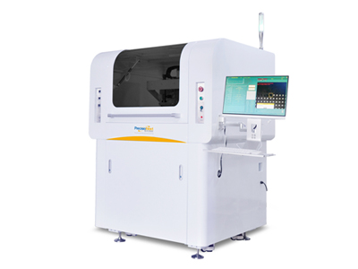
Semiconductor equipment refers to electrical equipment manufactured using semiconductor components. Semiconductor refers to a material with a conductivity between a conductor and an insulator at room temperature. Semiconductors are widely used in radio, television, and temperature measurement. For example, a diode is a device made of semiconductors. A semiconductor is a material whose conductivity can be controlled from an insulator to a conductor.
A small integrated IC can be divided into five industries, including IC design, raw materials, wafer foundry, machinery and equipment, and packaging testing, according to the stage division of the entire industrial chain from design to production. Semiconductor equipment is divided into: semiconductor pre process equipment (wafer process equipment), and semiconductor post process equipment (semiconductor sealing and testing equipment).
Wafer process equipment:
Single crystal furnace: Melt semiconductor raw materials, pull single crystals, and produce single crystal semiconductor wafers for subsequent production of semiconductor components.
Vapor phase epitaxial growth furnace: It provides a special processing process and natural environment for vapor phase epitaxial growth and development. It is completed on a single crystal, where the growth and development have a corresponding relationship with the single crystal phase. It provides basic advance preparation for the completion of the function of the single crystal precipitation. Vapor phase epitaxy is a unique processing process for organic chemical vapor deposition, in which the molecular structure of growth and development chromatography is sustained on a single crystal substrate and is associated with maintaining the orientation of the substrate.
Air oxidation furnace: It is an indispensable stage in the semiconductor production process to carry out air oxidation solutions for semiconductor raw materials, produce a prescribed air oxidation atmosphere, and complete the semiconductor estimation design scheme.
Semiconductor equipment
Magnetron sputtering stage: According to a closed electromagnetic field parallel to the target surface in bipolar magnetron sputtering, and the orthogonal and magnetic fields generated on the target surface, the secondary electrons are constrained in a special area of the target surface, completing the hydrolysis of high ion relative density and high efficiency energy, and the target molecules or molecular structures are deposited on the substrate by high-speed transmission magnetron sputtering to produce a plastic film.
Lithography machine: Evenly glue the surface of a semiconductor plate (silicon wafer), transfer the pattern on the mask free template, and temporarily "copy" the components or power circuit structure onto the silicon wafer.
Reflecting the software of the ion implantation system: Tablet computers release high-frequency operating voltages between electrical stages, resulting in more than 100 μ The ion layer with a thickness of m is placed in a high velocity ion collision style to complete chemical change ion implantation and physical collision, and to complete the production, processing, and formation of semiconductors.
Ion introduction machine: carry out inclusion on the surrounding area of the semiconductor surface.
Probe test bench: Conduct electrical testing based on the pad contact between the probe and semiconductor components to verify whether the performance parameters of the semiconductor comply with the design scheme characteristics.
Round crystal dicing machine: Cut round crystals into small pieces.
Semiconductor sealing and testing equipment:
According to statistics from China International Tendering Network, the overall localization rate of sealing and testing equipment does not exceed 5%, while the localization rate of individual sealing and testing production lines is only 1%, which is significantly lower than the overall localization rate of 10% - 15% of manufacturing equipment. Especially in the core equipment of packaging, the localization rate of IC grade solid crystal machines, wire bonding machines, and wafer grinding machines is close to zero.
Solid crystal machines: Including LED solid crystal machines, IC grade solid crystal machines, etc., Praxion Intelligent IC grade solid crystal machines have broken the monopoly of foreign brands, completely surpassing foreign brands in terms of speed, accuracy, and stability, and have been recognized by sealing and testing giants such as Huatian, UTAC, and China Resources Micro.
Wire bonders: Wire bonders generally refer to ultrasonic wire bonders, which can be divided into gold wire bonders, aluminum wire bonders, and copper wire bonders based on wire material.